


1.10G,8G,4G,3G,2.5G,1.25G,155m all rate
2.SFP+,XFP,SFP,SFF,CSFP,are customizable
3.Perfectly compatible with famous switch,ZTE HUAWEI etc
4.DDM
5.Choice from Single mode,muli-mode
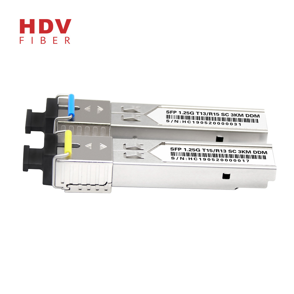
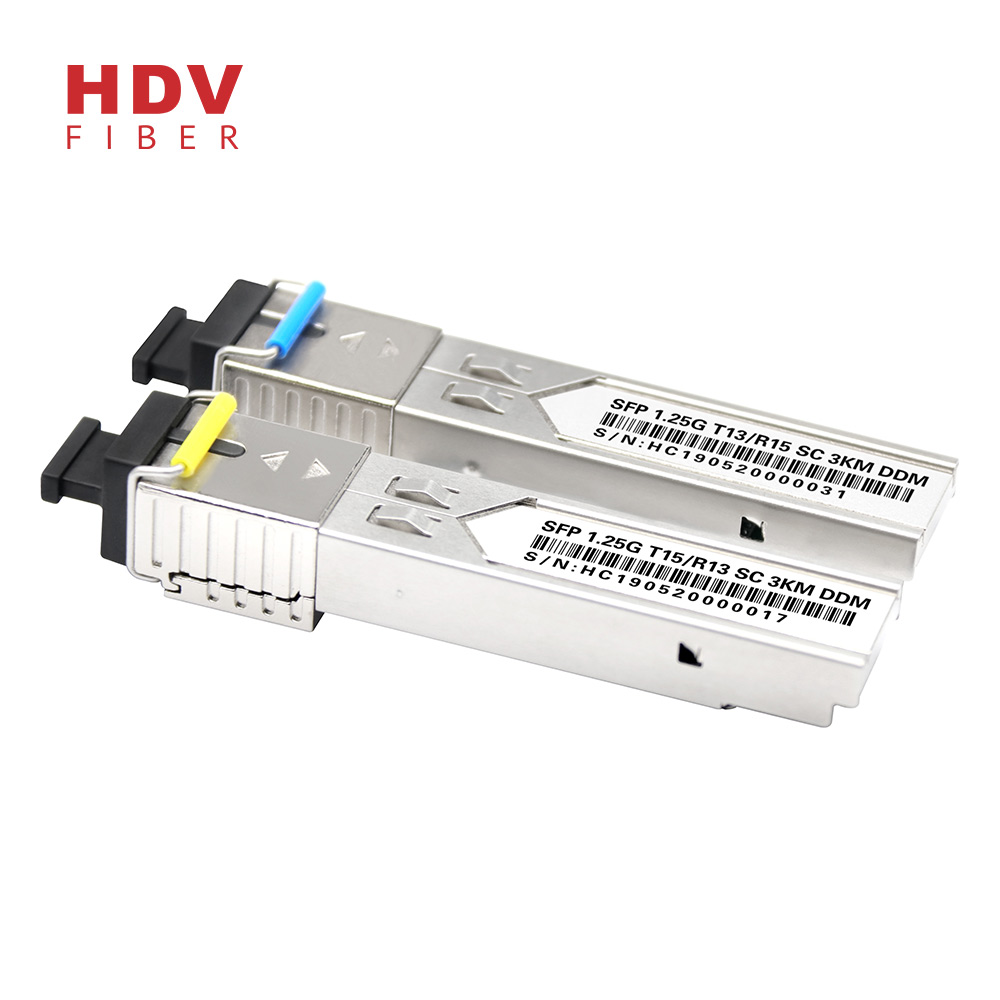
6.Choice from dual fiber LC,single fiber SC/LC
7.Low power consumption and high sensitivily
8.Programmable of no light alarm function
9.Complying with ROHS standard
10.The working temperature is up from -40c to ~+85c
11.Complying with Class 1 Laser,and the requirements of IEC60825-1
12.The label can be customized according to customer’s requirements
13.The excellent characteristic of overclocking
|
Brand |
OEM, ODM |
|
Place of origin |
China |
|
Condition |
New |
|
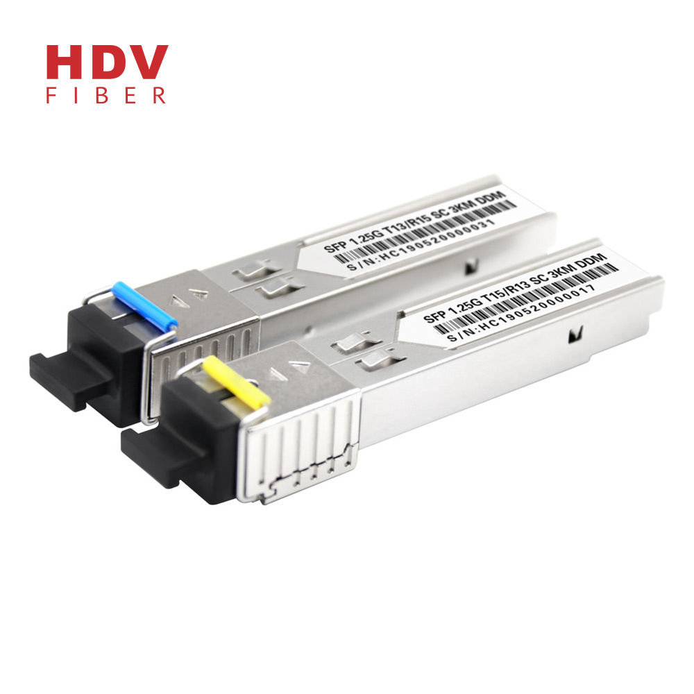
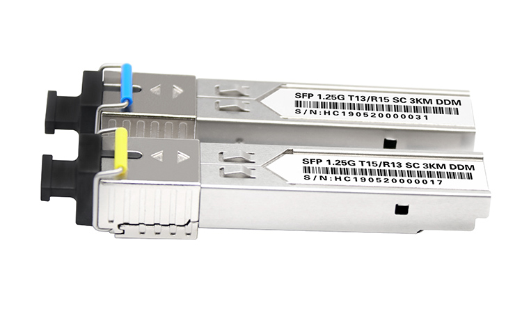
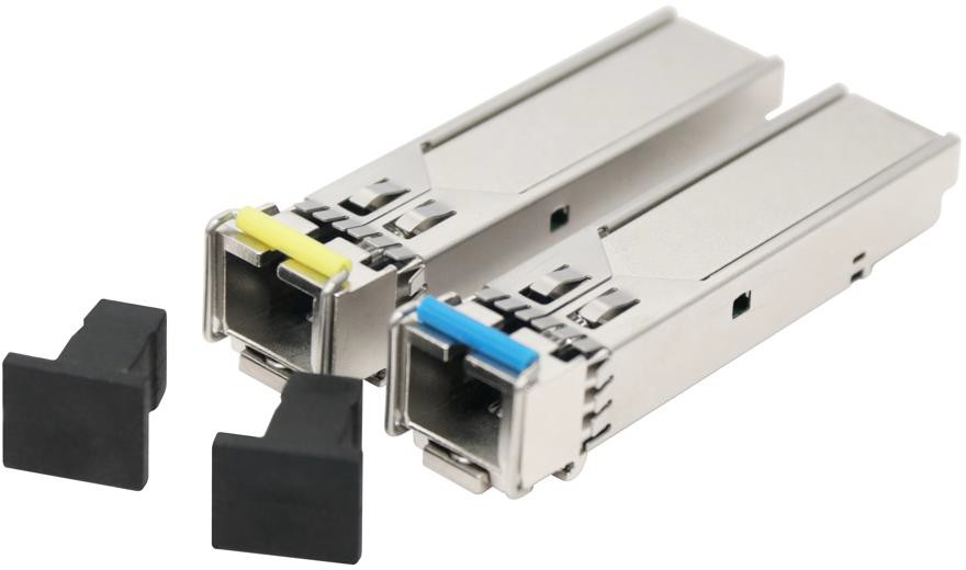
Form Factor |
SFP |
|
Wavelength: |
1310/1550nm |
|
Distance |
3KM |
|
Data Rate (max) |
1.25G |
|
Transmitter |
FP/DFB |
|
Receiver |
PIN |
|
Diagnostics |
Digital |
|
Low End Case Temperature (°C) |
0°C |
|
High End Case Temperature (°C) |
70°C |
|
Voltage Supply |
3.3v |
|
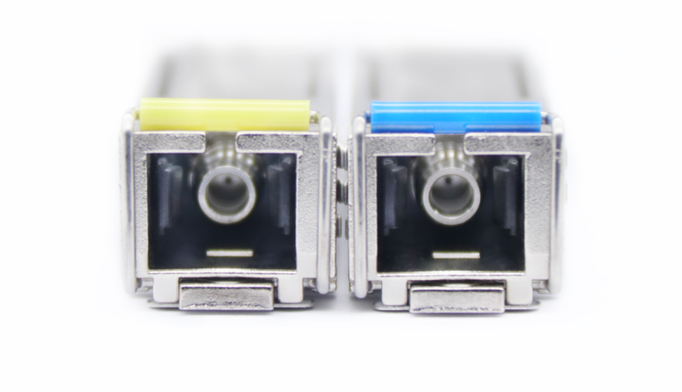
Connector |
SC |
|
Warranty |
2 year |
|
Compatible with |
ZTE ,HUAWEI, HP etc. |
|
Application |
Gigabit Ethernet/Fiber Channel |
|
Time of delivery |
2-4 working days |
|
Package |
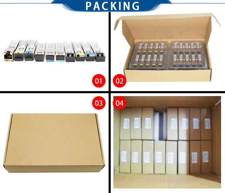
10 pcs/box |
1. Multi-sourced SFP package with singleSC/PC receptacle;
2. Single mode single fiber bi-directional transmission
3. Up to 10~120Km with 9/125μm SMF;
4. AC coupled for Rx and Tx side 5. Two temperature ranges: 0°C to +70°C for commercial level, -40°C to +85°C for industrial level;
6. Operates at data rate 1.25Gbps 7. Complies with MIL-STD-883/GR-468
1X fiber channel
Video monitor system
Telecommunication system
| Parameter | Symbol | Min | Max | Unit | |
| Storage Temperature | TS | -40 | +85 | ℃ | |
|
Operating Temperature
|
TOP |
Commercial level | -20 | +70 |
℃ |
| industrial level | -40 | 85 | |||
| Supply Voltage | VCC | -0.5 | +4.5 | V | |
| Voltage on Any Pin | VIN | 0 | VCC | V | |
| Soldering Temperature ,Time | - | 260℃, 10 S | ℃,S | ||
| Parameter | Symbol | Min. | Typ | Max. | Unit | |
|
Ambient Temperature |
TAMB |
Commercial level | 0 | - | 70 |
℃ |
| industrial level | -40 | 85 | ||||
| Power Supply Voltage | V CC-VEE | 3 | 3.3 | 3.6 | V | |
Transmitter(T=25℃, Vcc=3~3.6V (+3.3V))
| Parameter | Symbol | Min. | Typ | Max. | Unit | ||||
|
Center Wavelength |
lc |
1520 | 1550 | 1580 |
nm |
||||
| 1280 | 1310 | 1340 | |||||||
| 1470 | 1490 | 1510 | |||||||
|
Spectral width |
△l |
FP@RMS | - | 2 | 4 |
nm |
|||
| DFB@-20dB
FWHM |
- | - | 1 | ||||||
|
Output Power |
0~20km |
1.25G |
1310 FP |
Po |
-9 | - | -3 |
dBm |
|
| 14/15 DFB | -15 | -3 | |||||||
|
40km |
1.25G |
14/15 DFB | -9 | - | -3 | ||||
| 1310 DFB | -5 | -0 | |||||||
| 60km | 1.25G | 14/15 DFB | -5 |
0 |
|||||
| 80km | 1.25G | 14/15 DFB | -3 | 2 | |||||
| 100~120km | 1.25G | 14/150 DFB | 0 | 3 | |||||
| Extinction Ratio | ER | 9 | - |
dB |
|||||
| Supply Current | ICCT | - |
150 |
mA |
|||||
| Input Differential Impedance | Rin | 100 |
Ω |
||||||
| Data Input Swing Differential | Vin | 300 |
1200 |
mV |
|||||
| Optical Modulation Amplitude | OMA | 174 |
μW |
||||||
| Transmit Disable Voltage | VD | 2.0 |
Vcc |
V | |||||
| Transmit Enable Voltage | VEN | 0 |
0.8 |
V | |||||
| Transmit Disable Assert Time |
10 |
us |
|||||||
|
Optical Rise/Fall Time |
1.25G |
Tr/ Tf
(20-80%) |
150 |
260 |
ps |
||||
| Deterministic Jitter Contribution | TX ΔDJ | 20 |
56.5 |
ps |
|||||
| Total Jitter Contribution | TX ΔTJ | 50 |
119 |
ps |
|||||
Receiver (T=25℃, Vcc=3~3.6V (+3.3V)
| Parameter | Symbol | Min. | Typ |
Max. |
Unit | |||
|
Wavelength Range |
lc |
1520 | 1550 |
1580 |
nm |
|||
| 1280 | 1310 |
1340 |
||||||
| 1470 | 1490 |
1510 |
||||||
|
Sensitivity |
20km |
1.25G | Pin |
PMIN |
- | - |
-21 |
dBm |
|
40/60km |
1.25G | Pin | - | - | -24 | |||
|
80km |
1.25G | Pin | - | - | -26 | |||
|
100km |
1.25G | APD | -30 | |||||
|
120km |
1.25G | APD | -32 | |||||
| MAX. Input Power (Saturation) | PMAX | -3 | - | - | ||||
| Signal Detect Assert | PA | - | - | -24 | ||||
| Signal Detect De-assert | PD | -45 | - | - | ||||
| Signal Detect Hysteresis | PHYS | 1 | - | 4 | ||||
| Supply Current | ICCR | - | - |
150 |
mA | |||
| Data Output Swing Differential | Vout | 400 | - |
1000 |
mV | |||
| Signal Detect Voltage – High | VSDHC | 2.0 | - |
VCC |
V |
|||
| Signal Detect Voltage – Low | VSDL | 0 | - | 0.8 | ||||
Notes:
switch from a high state to a low state.
1)Value of output power and sensitivity can be customized according to the demand
|
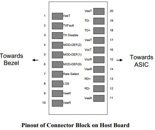
Pin |
Descriptions | Pin | Descriptions |
|
1 |
VEET | Transmitter Ground (Common with Receiver Ground) | 1 |
|
2 |
TFAULT | Transmitter Fault. | 2 |
|
3 |
TDIS | Transmitter Disable. Laser output disabled on high or open. | 3 |
|
4 |
MOD_DEF(2) | Module Definition 2. Data line for Serial ID. | 4 |
|
5 |
MOD_DEF(1) | Module Definition 1. Clock line for Serial ID. | 4 |
|
6 |
MOD_DEF(0) | Module Definition 0. Grounded within the module. | 4 |
|
7 |
Rate Select | No connection required | |
|
8 |
LOS | Loss of Signal indication. Logic 0 indicates normal operation. | 5 |
|
9 |
VEER | Receiver Ground (Common with Transmitter Ground) | 1 |
|
10 |
VEER | Receiver Ground (Common with Transmitter Ground) | 1 |
|
11 |
VEER | Receiver Ground (Common with Transmitter Ground) | 1 |
|
12 |
RD- | Receiver Inverted DATA out. AC Coupled | |
|
13 |
RD+ | Receiver Non-inverted DATA out. AC Coupled | |
|
14 |
VEER | Receiver Ground (Common with Transmitter Ground) | 1 |
|
15 |
VCCR | Receiver Power Supply | |
|
16 |
VCCT | Transmitter Power Supply | |
|
17 |
VEET | Transmitter Ground (Common with Receiver Ground) | 1 |
|
18 |
TD+ | Transmitter Non-Inverted DATA in. AC Coupled. | |
|
19 |
TD- | Transmitter Inverted DATA in. AC Coupled. | |
|
20 |
VEET | Transmitter Ground (Common with Receiver Ground) | 1 |
Notes:
1. Circuit ground is internally isolated from chassis ground.
2. TFAULTis an open collector/drain output, which should be pulled up with a 4.7k – 10k Ohms resistor on the host board if intended for use. Pull up voltage should be between 2.0V to Vcc + 0.3V. A high output indicates a transmitter fault caused by either the TX bias current or the TX output power exceeding the preset alarm thresholds. A low output indicates normal operation. In the low state, the output is pulled to <0.8V.
4. Laser output disabled on TDIS>2.0V or open, enabled on TDIS<0.8V.
5. Should be pulled up with 4.7k – 10 kohms on host board to a voltage between 2.0V and 3.6V. MOD_DEF(0) pulls line low to indicate module is plugged in.
6. LOS is open collector output. Should be pulled up with 4.7k – 10 kohms on host board to a voltage between 2.0V and 3.6V. Logic 0 indicates normal operation; logic 1 indicates loss of signal.
Example
SFP 35 24 -F 1 1 SC-20
| Sign | Mean | Description | ||||
| SFP | Module type | SFP=Single fiber SFP transceiver | ||||
| 35 | Center wave | 35=1310tx/1550rx | 53=1550tx/1310rx | 45=1490tx/1550rx | 54=1550tx/1490rx | |
| 24 | Transmitter Rate | 03=155M | 03=622M | 24=1.25G | 48=2.5G | 60=3.125G |
| F | Laser type | F=FP | D=DFB | C=CWDM | V=VCSEL | |
| 1 | Operating T | 1=0~+70℃ | 2=-40~+85℃ | |||
| 2 | DDMI | 1=NO DDM | 2=DDMI | |||
| LC | Connector | SC=SC | LC=LC | |||
|
20 |
Distance |
022=220M | 055=550M | 5=5KM | 10=10KM | |
| 20=20KM | 40=40KM | 80=80KM | 100=100KM | |||
|
Part No. |
Wavelength |
Connector |
Temp. |
TX Power (dBm) | RX Sens
(Max.) (dBm) |
Distance |
| SFP3524-F11SC-20 | T 1310FP/R 1550 | SC |
-20 to 70 |
-9 to-3 | -21 |
20km |
| SFP5324-D11SC-20 |
T 1550DFB/R 1310 |
SC |
-20 to 70 |
-15 to-3 | -21 | |
| SFP5324-D11SC-40 |
T 1550DFB/R 1310 |
SC |
-20 to 70 |
-9 to-3 | -24 |
40km |
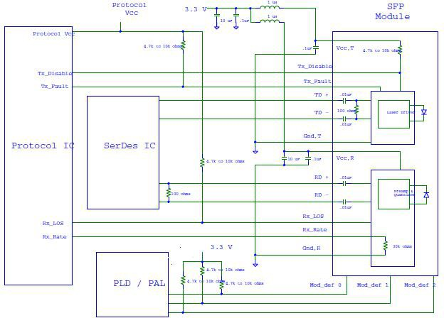
Figure 2 Example SFP Host Board Schematic
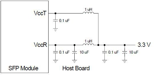
Figure 3 Recommended Host Board Supply Filtering Network
Small Form-factor Pluggable (SFP) Transceiver MultiSource Agreement (MSA)
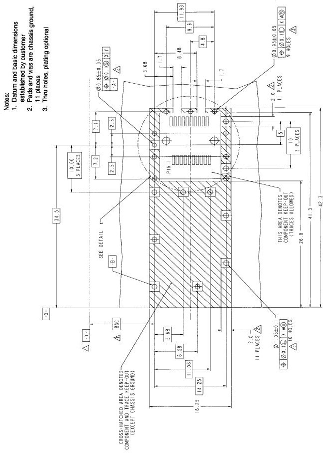
Figure 4 SFP Host Board Mechanical Layout
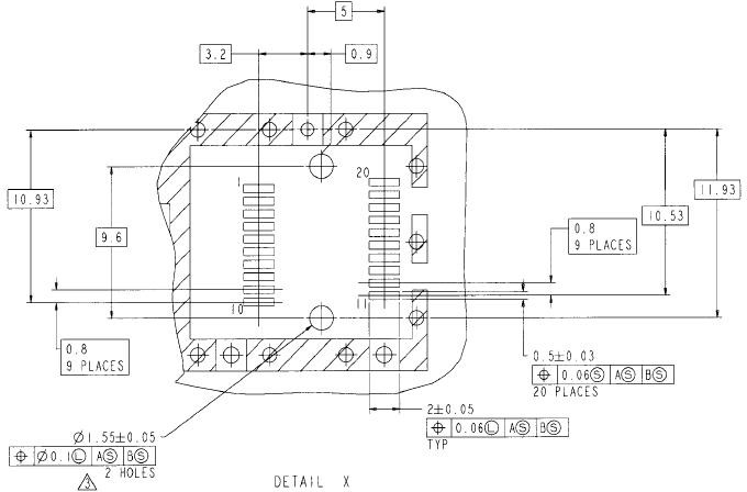
Figure 5 SFP Host Board Mechanical Layout (Cont.)
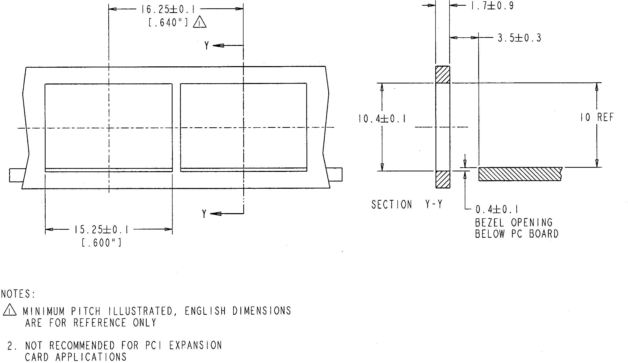
Figure 6 Recommended Bezel Design
| REV: | A |
| DATE: | August 30,2012 |
| Write by: | HDV phoelectron technology LTD |
| Contact: | Room703,Nanshan district science college town, Shenzhen, China |
| WEB: | Http://www.hdv-tech.com |
Products categories

Write your message here and send it to us