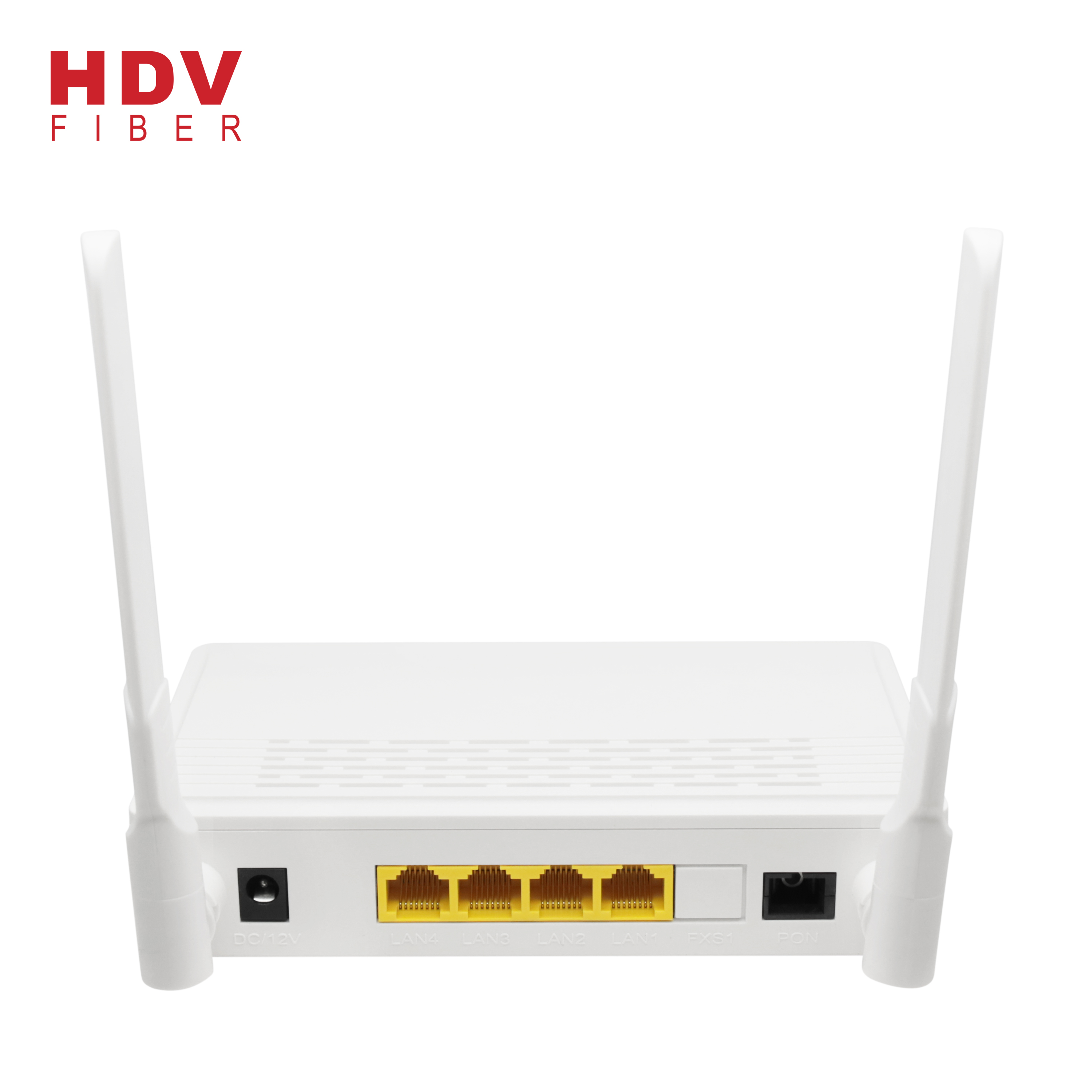
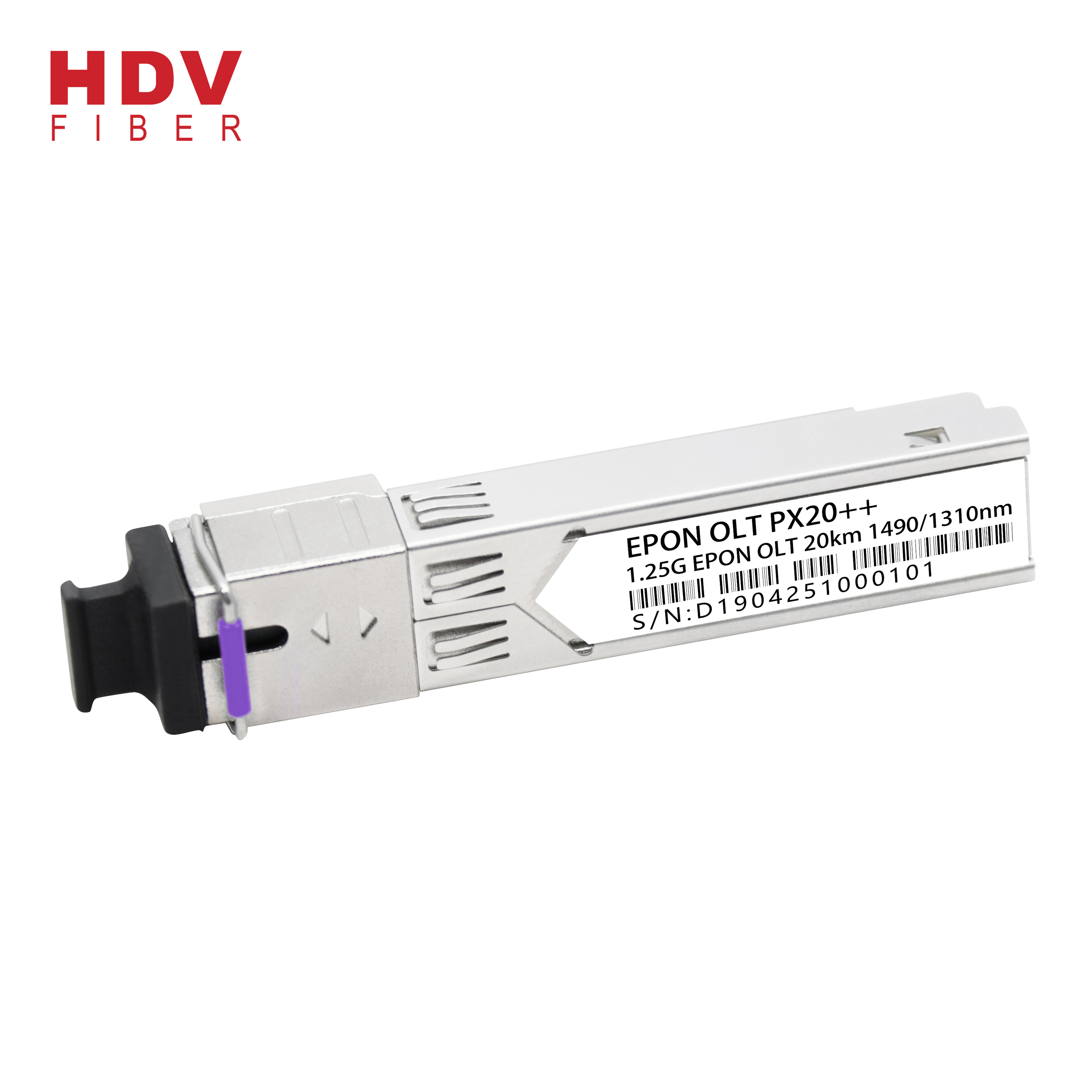
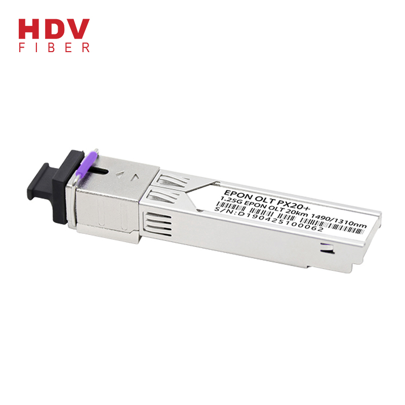
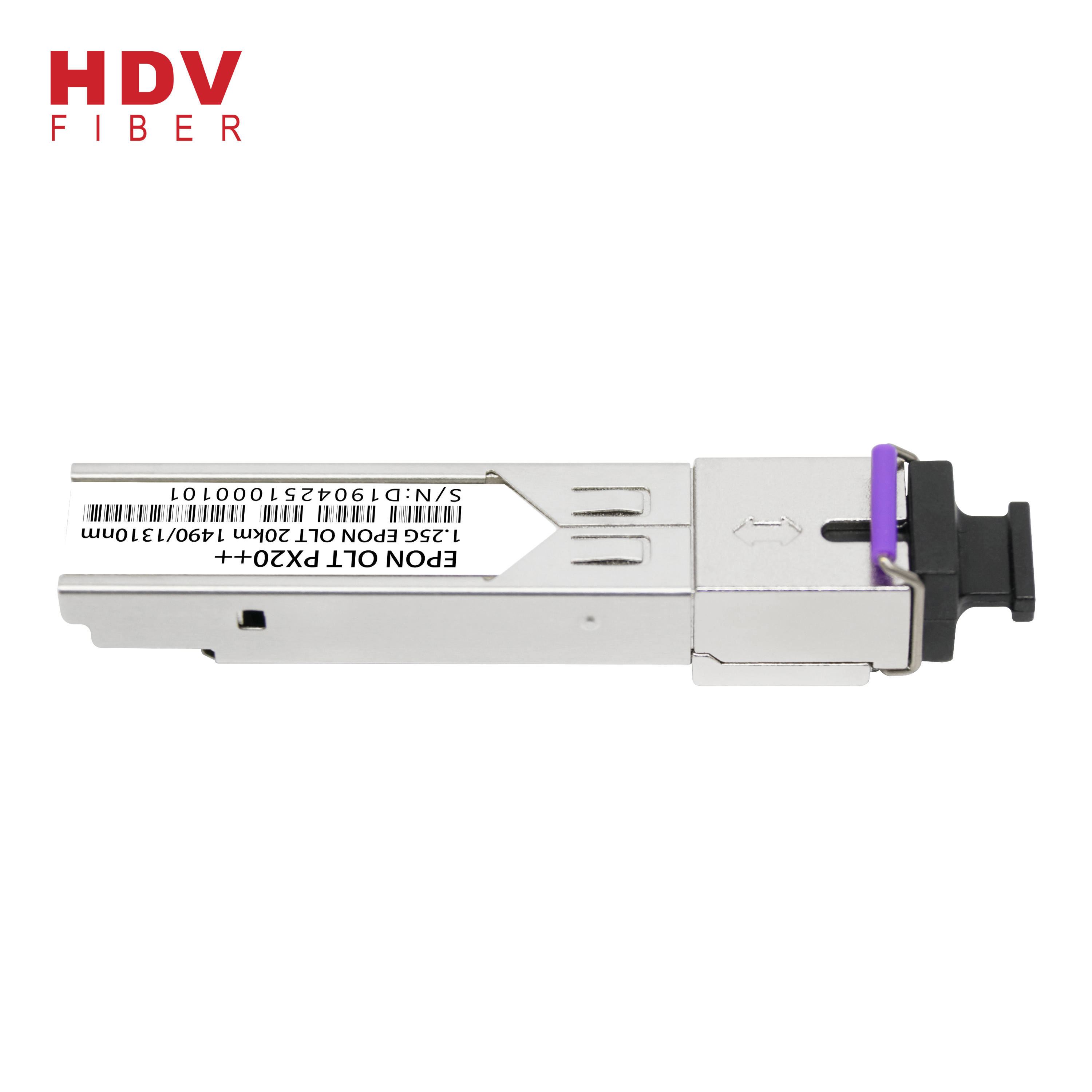
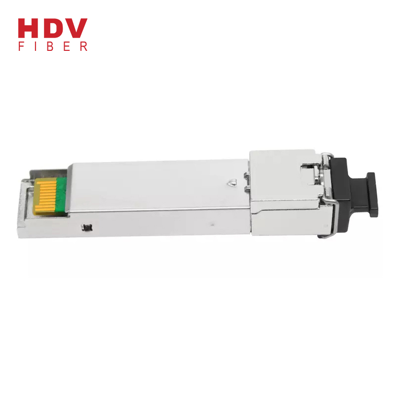
factory low price Onu Gpon Ftth - 1000BASE-PX20++ EPON OLT SFP Transceiver ZL5432099-ICS – HDV Detail:
Product Applications
GEPON OLT For P2MP Application
General
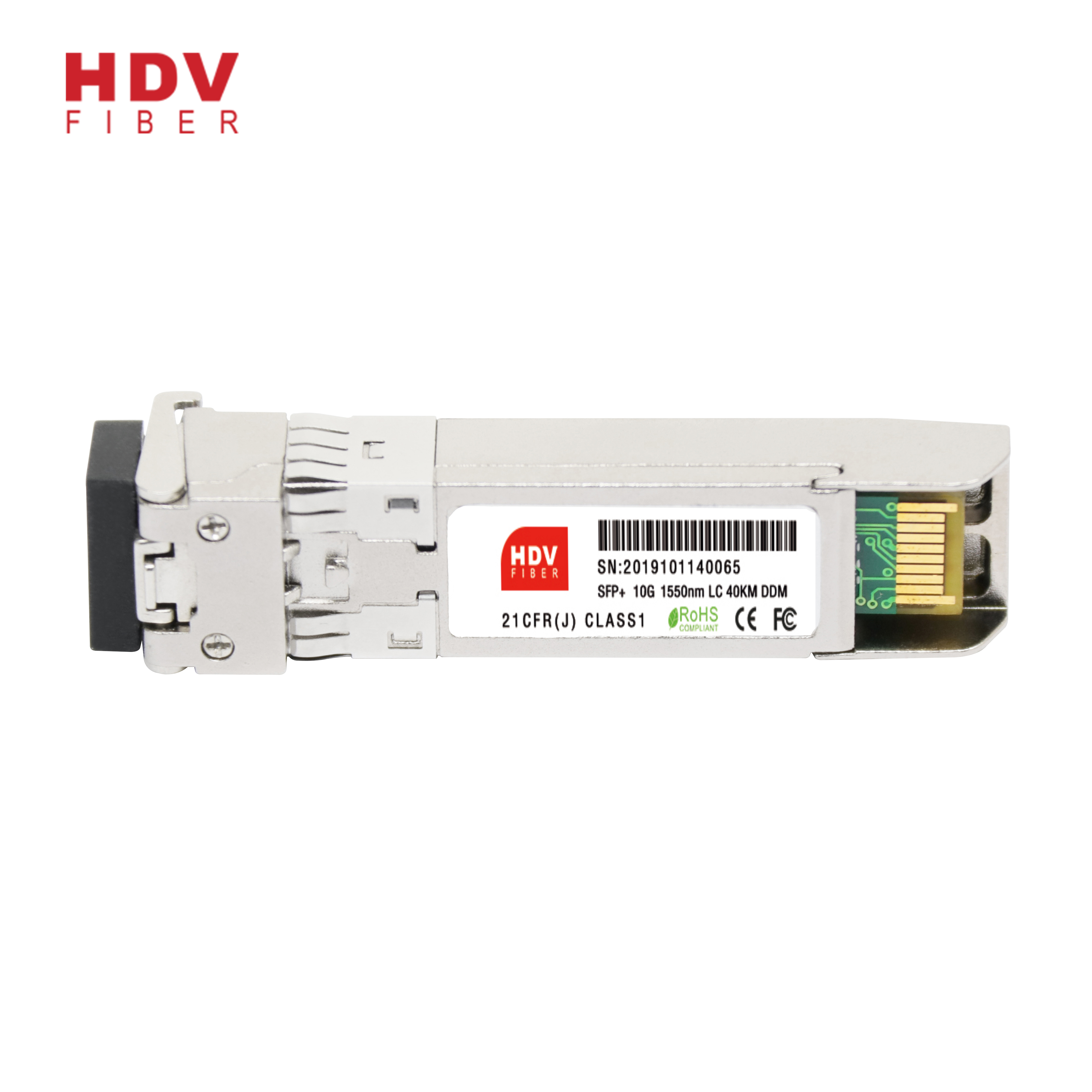
The HDV ZL5432099-ICS transceiver with supports data rate of typical 1.25 Gbps for GEPON OLT application up to 20km transmission distance, it’s designed meeting with China Telecom EPON equipment technical requirement V2.1 1000BASE-PX20+ specifications. SC rececptacle is for optical interface.
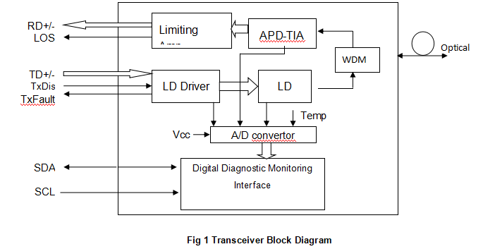
The module provides digital diagnostic information of its operating conditions and status, including transmitting power, laser bias, receiver input optical power, module temperature, and supply voltage. Calibration and alarm/warning threshold data are written and stored in internal memory (EEPROM). The memory map is compatible with SFF-8472, as shown in Fig. 2. The diagnostic data are raw A/D values and must be converted to real world units using calibration constants stored in EEPROM locations 56 – 95 in A2h.
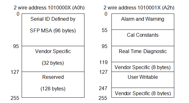
Fig 2 EEPROM Information
Performance Specifications
|
Absolute Maximum Ratings |
|||||||||||
|
Parameter |
Symbol |
Min. |
Max. |
Unit |
Note |
||||||
|
Storage Temperature
|
Tst |
-40 |
+85 |
°C |
|||||||
|
Operating Case Temperature |
Tc |
0 |
70 |
°C |
|||||||
|
Input Voltage |
- |
GND |
Vcc |
V |
|||||||
|
Power Supply Voltage |
Vcc-Vee |
-0.5 |
+3.6 |
V |
|||||||
| Recommended Operating Conditions | |||||||||||
|
Parameter |
Symbol |
Min. |
Typical |
Max. |
Unit |
Note | |||||
|
Power Supply Voltage |
Vcc |
3.135 |
3.3 |
3.465 |
V |
||||||
|
Operating Case Temperature |
Tc |
0 |
- |
70 |
°C |
||||||
|
Data Rate |
DR |
- |
1.25 |
- |
Gbps |
||||||
|
Total Supply Current |
- |
- |
- |
400 |
mA |
||||||
|
Damage Threshold For Receiver |
- |
- |
- |
4 |
dBm |
||||||
|
Optical Specification |
||||||
|
Transmitter |
||||||
|
Parameter |
Symbol |
Min. |
Typ. |
Max. |
Unit |
Note |
| Optical Central Wavelength |
l |
1480 |
1490 |
1500 |
nm |
- |
|
Spectral Width (-20dB) |
Dl |
- |
- |
1 |
nm |
- |
|
Side Mode Suppression Ratio |
SMSR |
30 |
- |
- |
dB |
- |
|
Average Optical Output Power |
Po |
+3 |
- |
+7 |
dBm |
- |
|
Extinction Ratio |
Er |
9 |
- |
- |
dB |
- |
|
Rise/Fall Time |
Tr/Tf |
- |
- |
260 |
ps |
- |
|
Transmitter Total Jitter |
Jp-p |
- |
- |
344 |
ps |
|
|
Transmitter Reflectance |
RFL |
- |
- |
-12 |
dB |
|
|
Average Lauched Power of Off Transmitter |
Poff |
- |
- |
-39 |
dBm |
- |
|
Differential Input Voltage |
VIN-DIF |
300 |
- |
1600 |
mV |
- |
|
Tx Disable Input Voltage-Low |
VIL |
0 |
- |
0.8 |
V |
- |
|
Tx Disable Input Voltage-High |
VIH |
2.0 |
- |
Vcc |
V |
- |
|
Output Eye |
Compliant with IEEE 802.3ah-2004 |
|||||
|
Receiver |
||||||
|
Parameter |
Symbol |
Min. |
Typ. |
Max. |
Unit |
Note |
|
Operate Wavelength |
- |
1280 |
1310 |
1340 |
nm |
- |
|
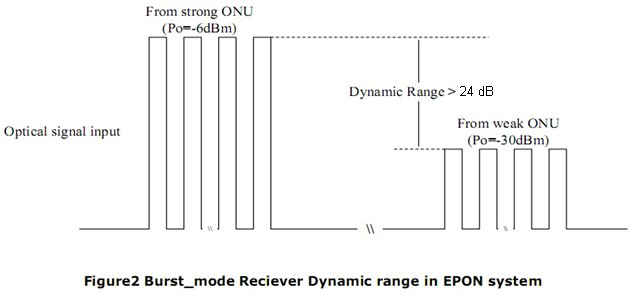
Sensitivity |
Pr |
- |
- |
-30 |
dBm |
1 |
|
Saturation |
Ps |
-6 |
- |
- |
dBm |
1 |
|
LOS assert Level |
- |
-45 |
- |
- |
dBm |
- |
|
LOS De-Assert Level |
- |
- |
- |
-30 |
dBm |
- |
|
LOS Hysteresis |
- |
0.5 |
- |
5 |
dB |
- |
|
Receiver Optical Reflectance |
- |
- |
- |
-12 |
dB |
- |
|
Data Output Low |
Vol |
-2 |
- |
-1.58 |
V |
- |
|
Data Output High |
Voh |
-1.1 |
- |
-0.74 |
V |
- |
|
LOSOutput Voltage-Low |
VSD-L |
0 |
- |
0.8 |
V |
- |
|
LOS Output Voltage-High |
VSD-H |
2.0 |
- |
Vcc |
V |
|
Note:
1. Minimum Sensitivity and saturation levels for an 8B10B 27-1 PRBS. BER≤10-12, 1.25Gpbs, ER=9dB
EEPROM Information
EEPROM Serial ID Memory Contents (A0h)
|
Addr. (decimal) |
Field Size (Bytes) |
Name of Field |
Content (Hex) |
Content (Decimal) |
Description |
|
0 |
1 |
Identifier |
03 |
3 |
SFP |
|
1 |
1 |
Ext. Identifier |
04 |
4 |
MOD4 |
|
2 |
1 |
Connector |
01 |
1 |
SC |
|
3-10 |
8 |
Transceiver |
00 00 00 80 00 00 00 00 |
00 00 00 128 00 00 00 00 |
EPON |
|
11 |
1 |
Encoding |
01 |
1 |
8B10B |
|
12 |
1 |
BR, nominal |
0C |
12 |
1.25Gbps |
|
13 |
1 |
Reserved |
00 |
0 |
- |
|
14 |
1 |
Length (9um)-km |
14 |
20 |
20/km |
|
15 |
1 |
Length (9um) |
C8 |
200 |
20km |
|
16 |
1 |
Length (50um) |
00 |
0 |
- |
|
17 |
1 |
Length (62.5um) |
00 |
0 |
- |
|
18 |
1 |
Length (copper) |
00 |
0 |
- |
|
19 |
1 |
Reserved |
00 |
0 |
- |
|
20-35 |
16 |
Vendor name |
48 44 56 20 20 20 20 20 20 20 20 20 20 20 20 20 |
90 45 81 85 73 67 75 32 32 32 32 32 32 32 32 32 |
HDV (ASCII) |
|
36 |
1 |
Reserved |
00 |
0 |
- |
|
37-39 |
3 |
Vendor OUI |
00 00 00 |
0 0 0 |
- |
|
40-55 |
16 |
Vendor PN |
5A 4C 35 34 33 32 30 39 39 2D 49 43 53 20 20 20 |
90 76 53 52 51 50 48 57 57 45 73 67 83 32 32 32 |
‘ZL5432099-ICS’ (ASCII) |
|
56-59 |
4 |
Vendor rev |
30 30 30 20 |
48 48 48 32 |
“000” (ASCII) |
|
60-61 |
2 |
Wavelength |
05 D2 |
05 210 |
1490 |
|
62 |
1 |
Reserved |
00 |
0 |
- |
|
63 |
1 |
CC BASE |
- |
- |
Check sum of bytes 0 – 62 |
|
64 |
1 |
Reserved |
00 |
0 |
|
|
65 |
1 |
Options |
1A |
26 |
|
|
66 |
1 |
BR, max |
00 |
0 |
- |
|
67 |
1 |
BR, min |
00 |
0 |
- |
|
68-83 |
16 |
Vendor SN |
- |
- |
ASCII |
|
84-91 |
8 |
Vendor date |
- |
- |
Year (2 bytes), Month (2 bytes), Day (2 bytes) |
|
92 |
1 |
DDM Type |
68 |
104 |
Internal Calibrated |
|
93 |
1 |
Enhanced Option |
B0 |
176 |
LOS, TX_FAULT and Alarm/warning flags implemented |
|
94 |
1 |
SFF-8472 Compliance |
03 |
3 |
SFF-8472 Rev 10.3 |
|
95 |
1 |
CC EXT |
- |
- |
Check sum of bytes 64 – 94 |
|
96-255 |
160 |
Vendor spec |
Alarm and Warning Thresholds (Serial ID A2H)
|
Parameter(Unit) |
C Temp |
Voltage |
Bias |
TX Power |
RX Power |
|
High Alarm |
100 |
3.6 |
90 |
+7 |
-6 |
|
Low Alarm |
-10 |
3 |
0 |
+2 |
-30 |
|
High Warning |
95 |
3.5 |
70 |
+6 |
-7 |
|
Low Warning |
0 |
3.1 |
0 |
+3 |
-29 |
Digital Diagnostic Monitor Accuracy
| Parameter | Unit | Accuracy |
Range |
Calibration |
|
Tx Optical Power |
dB |
±3 |
Po: -Pomin~Pomax dBm, Recommended operation conditions |
External/Internal |
|
Rx Optical Power |
dB |
±3 |
Pi: Ps~Pr dBm, Recommended operation conditions |
External/Internal |
|
Bias Current |
% |
±10 |
Id: 1-100mA, Recommended operating conditions |
External/Internal |
|
Power Supply Voltage |
% |
±3 |
Recommended operating conditions |
External/Internal |
|
Internal Temperature |
℃ |
±3 |
Recommended operating conditions |
External/Internal |
|
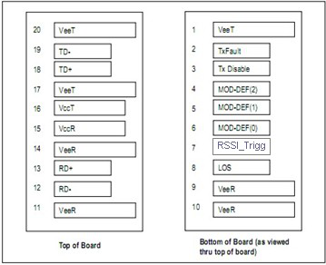
Pin No. |
Name |
Function |
Plug Seq. |
Notes |
|
1 |
VeeT |
Transmitter Ground |
1 |
|
|
2 |
Tx Fault |
Transmitter Fault Indication |
3 |
Note 1 |
|
3 |
Tx Disable |
Transmitter Disable |
3 |
Note 2 |
|
4 |
MOD-DEF2 |
Module Definition 2 |
3 |
Note 3 |
|
5 |
MOD-DEF1 |
Module Definition 1 |
3 |
Note 3 |
|
6 |
MOD-DEF0 |
Module Definition 0 |
3 |
Note 3 |
|
7 |
RSSI_Trigg |
Receiver Signal Strength Indication |
3 |
|
|
8 |
LOS |
Los Of Signal |
3 |
Note 4 |
|
9 |
VeeR |
Receiver Ground |
1 |
Note 5 |
|
10 |
VeeR |
Receiver Ground |
1 |
Note 5 |
|
11 |
VeeR |
Receiver Ground |
1 |
Note 5 |
|
12 |
RD- |
Inv. Receiver Data Out |
3 |
Note 6 |
|
13 |
RD+ |
Receiver Data Out |
3 |
Note 6 |
|
14 |
VeeR |
Receiver Ground |
1 |
Note 5 |
|
15 |
VccR |
Receiver Power Supply |
2 |
Note 7, 3.3V± 5% |
|
16 |
VccT |
Transmitter Power Supply |
2 |
Note 7, 3.3V± 5% |
|
17 |
VeeT |
Transmitter Ground |
1 |
Note 5 |
|
18 |
TD+ |
Transmitter Data In |
3 |
Note 8 |
|
19 |
TD- |
Inv.Transmitter Data In |
3 |
Note 8 |
|
20 |
VeeT |
Transmitter Ground |
1 |
Note 5 |
Notes:
- TX Fault is an open collector/drain output, which should be pulled up with a 4.7K–10KΩ resistor on the host board. Pull up voltage between 2.0V and VccT, R+0.3V. When high, output indicates a laser fault of some kind. Low indicates normal operation. In the low state, the output will be pulled to < 0.8V.
- TX disable is an input that is used to shut down the transmitter optical output. It is pulled up within the module with a 4.7–10 KΩ resistor. Its states are:
Low (0 – 0.8V): Transmitter on
(>0.8, < 2.0V): Undefined
High (2.0 – 3.465V): Transmitter Disabled
Open: Transmitter Disabled
- Mod-Def 0,1,2. These are the module definition pins. They should be pulled up with a 4.7K – 10KΩ resistor on the host board. The pull-up voltage shall be VccT or VccR.
Mod-Def 0 is grounded by the module to indicate that the module is present
Mod-Def 1 is the clock line of two wire serial interface for serial ID
Mod-Def 2 is the data line of two wire serial interface for serial ID
4. LOS (Loss of Signal) is an open collector/drain output, which should be pulled up with a 4.7K – 10KΩ resistor. Pull up voltage between 2.0V and VccT, R+0.3V. When high, this output indicates the received optical power is below the worst-case receiver sensitivity (as defined by the standard in use). Low indicates normal operation. In the low state, the output will be pulled to < 0.8V.
- VeeR and VeeT may be internally connected within the SFP module.
- RD-/+: These are the differential receiver outputs. They are DC coupled 100Ω differential lines which should be terminated with 100Ω (differential) at the user SERDES.
- VccR and VccT are the receiver and transmitter power supplies. They are defined as 3.3V ±5% at the SFP connector pin. Maximum supply current is 450mA. Recommended host board power supply filtering is shown below. Inductors with DC resistance of less than 1Ω should be used in order to maintain the required voltage at the SFP input pin with 3.3V supply voltage. When the recommended supply filtering network is used, hot plugging of the SFP transceiver module will result in an inrush current of no more than 30 mA greater than the steady state value. VccR and VccT may be internally connected within the SFP transceiver module.
- TD-/+: These are the differential transmitter inputs. They are AC-coupled, differential lines with 100Ω differential termination inside the module. The AC coupling is done inside the module and is thus not required on the host board.
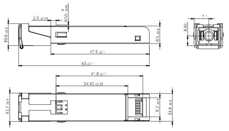
Package Diagram
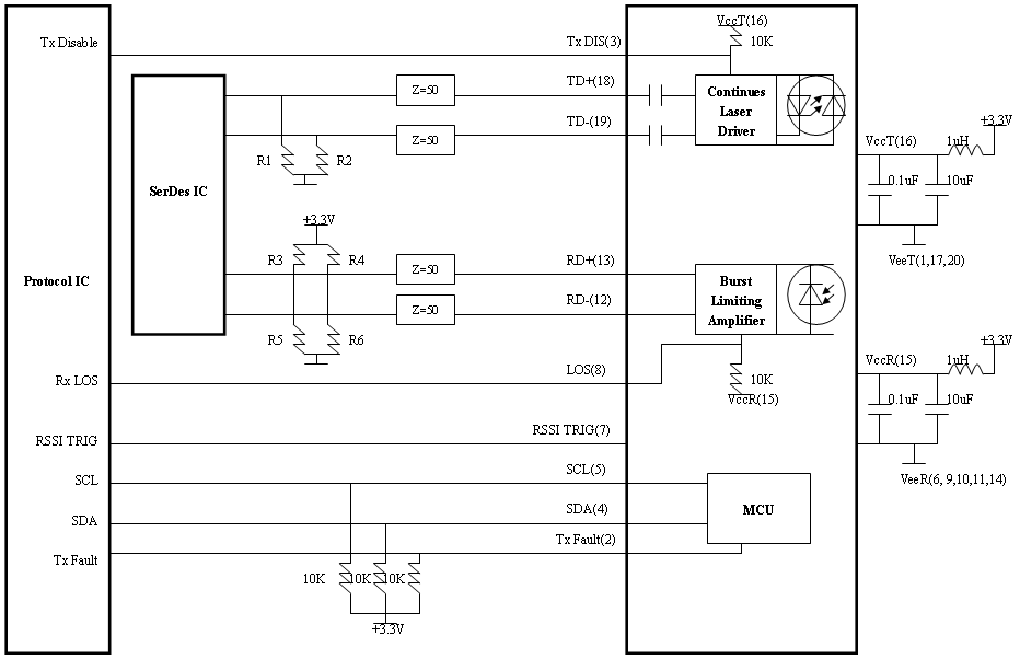
Recommended Circuit
Note:
Tx:AC coupled internally.
R1=R2=150Ω.
Rx: LVPECL output, DC coupled internally.
Input stage in SerDes IC with internal bias to Vcc-1.3V
R3=R4=R5=R6=N.C
Input stage in SerDes IC without internal bias to Vcc-1.3V
R3=R4=130Ω, R5=R6=82Ω.
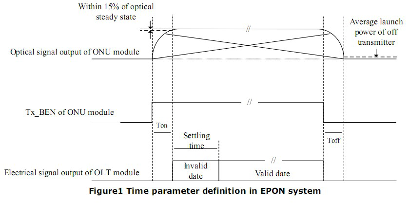
Timing Parameter Definition
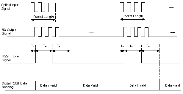
Timing Of Digital RSSI
|
PARAMETER |
SYMBOL |
MIN |
TYP |
MAX |
UNITS |
|
Packet Length |
- |
600 |
- |
- |
ns |
|
Trigger delay |
Td |
100 |
- |
- |
ns |
|
RSSI Trigger and Sample Time |
Tw |
500 |
- |
- |
ns |
|
Internal delay |
Ts |
500 |
- |
- |
us |
Change History
|
Version |
Change Description |
Issued By |
Checked By |
Appoved By |
Release Date |
|
A |
Initial release |
2016-01-18 |
| REV: | A |
| DATE: | August 30,2012 |
| Write by: | HDV phoelectron technology LTD |
| Contact: | Room703,Nanshan district science college town, Shenzhen, China |
| WEB: | Http://www.hdv-tech.com |
Product detail pictures:

Related Product Guide:
Six-port network appliance runs Linux on Atom C3558 | Sfp Gpon Onu
Open Eye MSA: Mit PAM 4 und bis zu 400 GBit/s durch das Rechenzentrum | Module Sfp
To get the stage of realizing dreams of our employees! To build a happier, more united and much more skilled crew! To reach a mutual benefit of our prospects, suppliers, the society and ourselves for factory low price Onu Gpon Ftth - 1000BASE-PX20++ EPON OLT SFP Transceiver ZL5432099-ICS – HDV , The product will supply to all over the world, such as: Juventus, Senegal, Mombasa, With nearly 30 years' experience in business, we are confident in superior service, quality and delivery. We warmly welcome customers from all over the world to cooperate with our company for common development.
In our cooperated wholesalers, this company has the best quality and reasonable price, they are our first choice.


