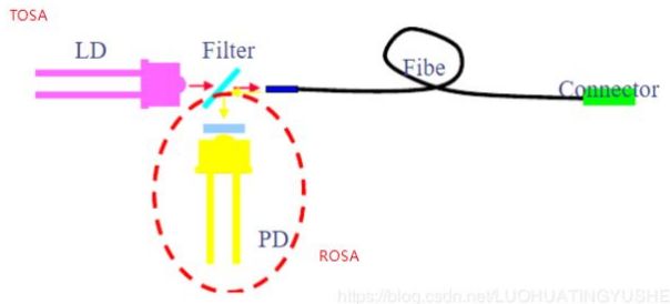
Composition of BOSA:
The light emitting part is called TOSA;
The light receiving part is called ROSA;
When two come together, they are called BOSA.
Electric to Optical TOSA:
LD (Laser Diode) semiconductor laser, used to convert electrical signals into optical signals for use in optical emission terminals
Optical to Electric ROSA:
PD Photo Dioder photodiode, used to convert light signals into current, which is then converted into a voltage signal through a mutual impedance amplifier (TIA).
TOSA and ROSA can be separately used as LC optical module and SC optical module. When BOSA is used, it is generally used as SC optical module
The selection of via size is based on the actual current size and has the following experience:
A 10mil hole with a 20mil PAD corresponds to a current of 0.5A for a 20mil wire, and a 40mil hole with a 40mil PAD corresponds to a current of 1A for a 40mil wire. When the current demand is high, multiple vias can be placed in adjacent positions to increase the bearing capacity. The drilling cost usually accounts for 30% to 40% of the PCB manufacturing cost.
Considering both cost and signal quality, it is better to choose 10/20mil (drilling/soldering pad) for 6-10 layer boards. For high-density and small-sized PCBs, 8mil drilling can be attempted. The small drilling size makes it difficult to achieve the process, the drill bit is easy to break, and the cost increases. Generally, board factories require drilling fees to be charged for drilling less than 11.81mil.
From a design perspective, a through hole includes the middle drilling hole and the surrounding solder pad, which determine the size of the drilling hole. As the size of the through hole is smaller, the parasitic capacitance is smaller, which is more conducive to the stability of high-speed signals
At the same time, the size of the through-hole is limited by the drilling process and electroplating process; The smaller the hole, the longer the time it takes, and the easier it is to deviate from the center position. When the drilling depth (through hole depth of about 50mil) exceeds 6 times the aperture, it is impossible to ensure uniform copper plating on the hole wall. Therefore, the minimum drilling diameter that PCB manufacturers can provide is 8mil.
The above is a brief overview of "Introduction to Key Parameters of BOSA - via size (I)", which can serve as a reference for everyone. Our company has a strong technical team and can provide professional technical services to customers. At present, our company has diversified products: intelligent onu, communication optical module, optical fiber module, sfp optical module, olt equipment, Ethernet switch and other network equipment. If you need, you can learn more about them.


