1. BOB commissioning process:
1. BOB commissioning process of HDV Phoelectron Technology LTD:
It is mainly to debug the optical power and eye map extinction ratio of the transmitting end, and the receiver needs to calibrate its sensitivity and RSSI monitoring.
BOB commissioning index:
| test | parameter | specifications | unit | remarks | |||
| function | attribute | description | Min. | Typ. | Max | ||
| Debugging part | TxPower | Tx transmitting power | 1.2 | 1.5 | 1.8 | dBm | For the specific measurement, the index can be optimized according to the BOSA performance |
| ExtRatio | extinction ratio | 9.5 | 12 | 14 | dB | ||
| EyeCross | eye diagram intersection | 45 | 50 | 55 | % | ||
| RxPoCalPoint_0 | The Rx calibration the first parameter condition | -10 | -10 | -10 | dB | ||
| RxPoCalPoint_1 | Rx calibration the second parameter condition | -20 | -20 | -20 | dB | ||
| RxPoCalPoint_2 | The Rx calibration the third parameter condition | -30 | -30 | -30 | dB | ||
| Testing part | TxPower | Tx transmitting power | 0.5 | 2.5 | 4 | dBm | For the specific measurement, the index can be optimized according to the BOSA performance |
| TxPo_DDM | Transmitting monitoring optical power | 0.5 | 2.5 | 4 | dB | ||
| DiffTxPower | Transmitting monitoring optical power difference | -1 | 0 | 1 | % | ||
| ExtRatio | Emission extinction ratio | 9 | 11 | 14 | dB | For the specific measurement, the index can be optimized according to the BOSA performance | |
| EyeCross | eye diagram intersection | 45 | 50 | 55 | dB | ||
| EyeMargin | Eye Diagram Magin | 10 | 10 | 10 | dB | ||
| TxCurrent | emission current | 180 | |||||
| TotalCurrent | total current | 100 | 250 | 300 | |||
| Sensitivity | sensitivity | -27 | -27 | ||||
2. BOB connection diagram of HDV Phoelectron Technology LTD.:
Conventional BOB test connection diagram, single-way test, complex external connection, the attenuator, error meter, power meter, CDR and other equipment need to be purchased separately. Each workstation requires a computer to support the test.
1. Introduction of ES-BOBT8 series BOB test equipment:
2. Can support up to 8 channels for BOB test, Internal integrated power meter and attenuator, can complete the sending and receiving debugging and test at the same time;
3. Integrated BERT function and 2xSFP + light source interface, can support 1.25G~10G optical signal output, to provide signal light source for BOB sensitivity test;
4. Integrated CDR Trigger out, internal self-built clock signal recovery, can provide the clock signal required for the optical eye diagram test;
5. Self-contained calibration power meter can provide standard optical power calibration detection.
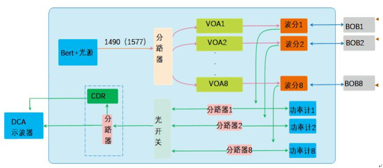
ES-BOBT8 series BOB test system provides a complete set of test equipment solutions, which can provide a maximum of 8 channels of ONU BOB test. The BER tester and light source, attenuator, power meter, wavelength division, optical switch and other equipment are integrated into one device , with professional BOB test automation software, can provide a complete set of BOB test solutions.
2、 Hardware working principle:
Role of the ES-BOBT8 series of BOB hardware systems:
1.In the production process, check whether the ONU optical port luminous power is normal in real time
2.Check whether the received optical power value read by the ONU optical port is accurate.
Working principle of the hardware system:
1. The upper computer software in the operating system is connected to the USB interface of the SCM U1 (model C8051F340) through the USB interface in the test system to realize man-machine interconnection;
2. The SCM U1 (model C8051F340) manages U3 (bit error detector chip VSC8228, signal generator), OLT module (PON SFP), ADC (implemented by ADL5303 and AD5593), and DAC (implemented by MAX4230 and AD5593) through the IIC bus.
3. The bit error detector chip VSC8228 sends out the signal of the specified code type and rate according to the instruction, and drives the OLT module to send out the optical signal of the corresponding code type and rate through the SerDES interface. The wavelength of the OLT sent out is 1490nm, and the light is divided into eight through the splitter. After the DAC control attenuator VOA attenuates to the specified optical power, it is connected to the ONU optical port. ONU reads the corresponding optical power and compares it with the actual value.
4. DAC implementation mechanism: SCM U1 (model C8051F340) sends DAC data to AD5593 through I2C bus, an I/O port of AD5593 generates an electrical signal, and a voltage signal is generated through the operational amplifier MAX4230, which is applied to the voltage input pin of the VOA attenuator , so that the light emitted by the PON OLT module is attenuated to the specified optical power, and then connected to the optical port of the ONU.
5. ADC implementation mechanism: After the light emitted by the ONU is detected by the PD (photodetector), the PD generates signal currents of different sizes according to the strength of the optical signal, and is converted into a voltage with a wider numerical range and higher precision through the logarithmic converter ADL5303. The value is recognized by AD5593 and converted into a digital signal through the I2C bus through the SCM U1 (model C8051F340) and finally presented on the host computer interface.


