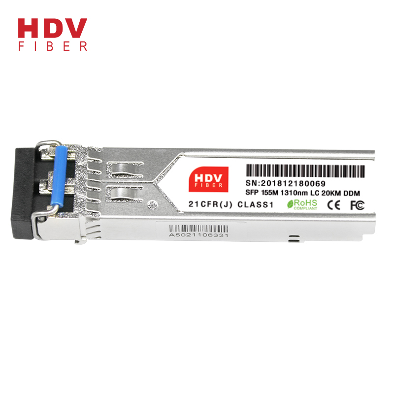
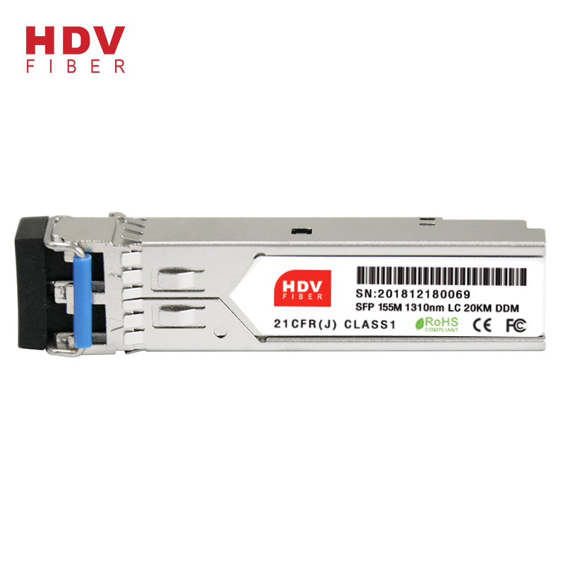
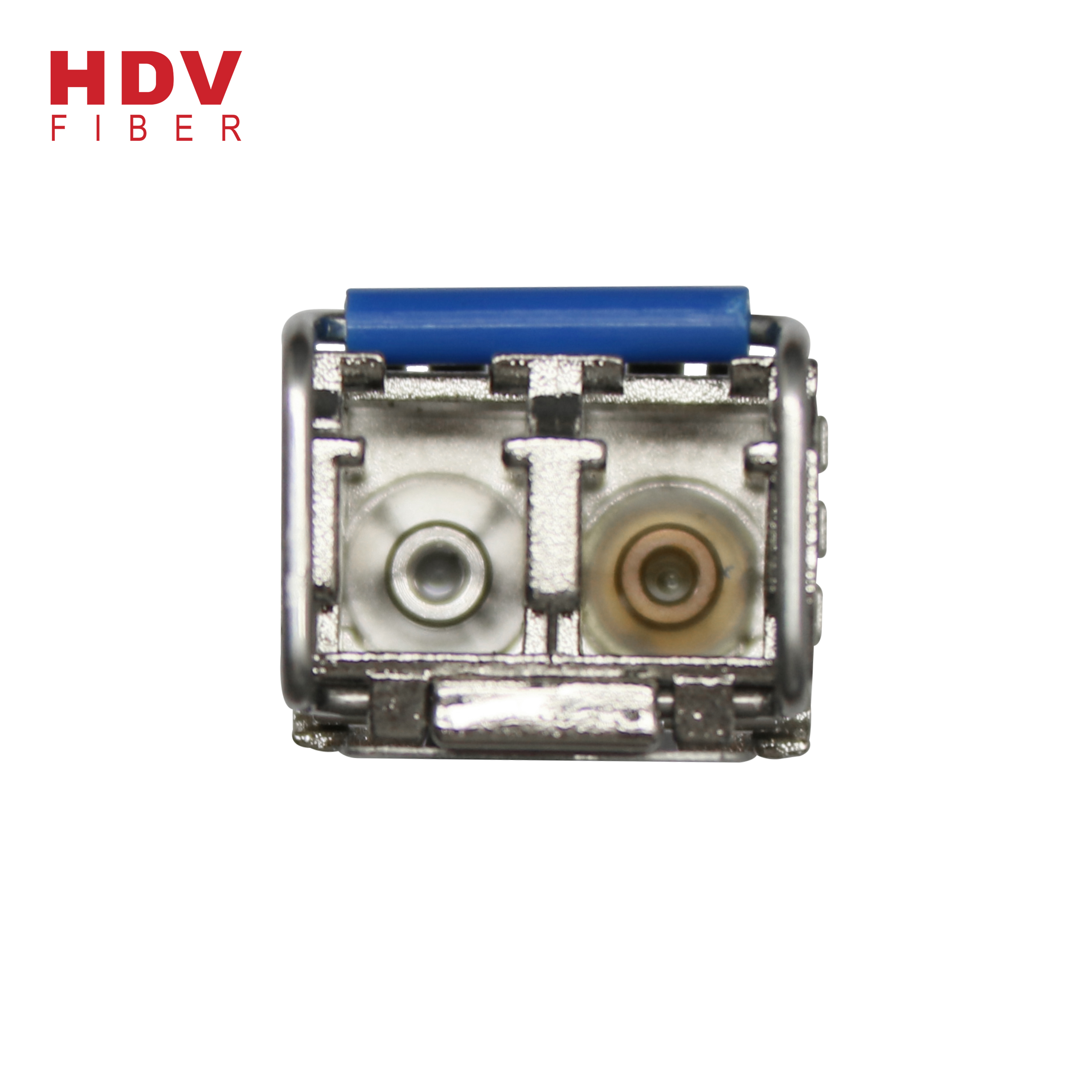
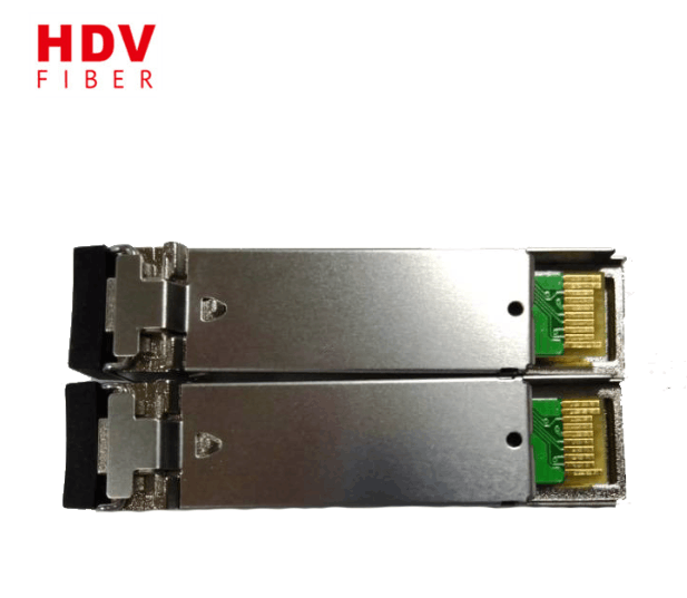
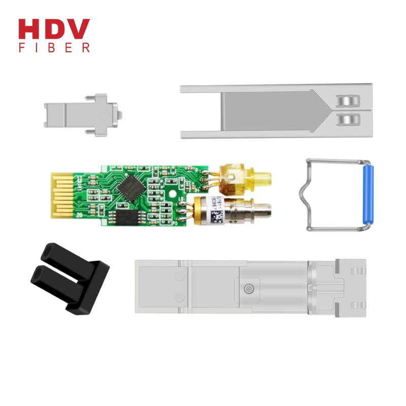
Single Core Sfp Module - 155m Lc 1310nm Dual Fiber 20km Fiber Optic Transceiver Sfp Module – HDV Detail:
Applications
Switch
Video monitor system Telecommunication system
Absolute Maximum Ratings
| Parameter | Symbol | Min | Max | Unit | |
| Storage Temperature | TS | -40 | +85 | ℃ | |
| Operating Temperature | TOP | Commercial level | -20 | +70 | ℃ |
| industrial level | -40 | 85 | |||
| Supply Voltage | VCC | -0.5 | +4.5 | V | |
| Voltage on Any Pin | VIN | 0 | VCC | V | |
| Soldering Temperature ,Time | - | 260℃, 10 S | ℃,S | ||
Recommended Operating Conditions
| Parameter | Symbol | Min. | Typ | Max. | Unit | |
| Ambient Temperature | TAMB | Commercial level | 0 | - | 70 | ℃ |
| industrial level | -40 | 85 | ||||
| Power Supply Voltage | V CC-VEE | 3 | 3.3 | 3.6 | V | |
Operating Conditions
1 Transmitter(T=25℃, Vcc=3~3.6V (+3.3V)) 155M
| Parameter | Symbol | Min. | Typ | Max. | Unit | |||
| Center Wavelength | FP | 1280 | 1310 | 1340 | ||||
| Spectral width | △l | FP@RMS | - | 4 | 6 | nm | ||
| Side Mode Suppression Ratio | SMSR (DFB only) | 30 | dB | |||||
| Output Power | 0~30km | 1310 FP | Po | -12 | - | -0 | dBm | |
| Extinction Ratio | ER | 155M | 10 | - | dB | |||
| Supply Current | ICCT | - | 150 | mA | ||||
| Input Differential Impedance | Rin | 100 | Ω | |||||
| Data Input Swing Differential | Vin | 300 | 1200 | mV | ||||
| Optical Modulation Amplitude | OMA | 174 | μW | |||||
| Transmit Disable Voltage | VD | 2.0 |
Vcc |
V | |
| Transmit Enable Voltage | VEN | 0 |
0.8 |
V | |
| Transmit Disable Assert Time |
10 |
us | |||
| Optical Rise/Fall Time | Tr/ Tf (20-80%) | 400 |
8000 |
ps | |
| Output Optical Eye | IUT-T G.957 Compliant | ||||
2 Receiver (T=25℃, Vcc=3~3.6V (+3.3V) 155M
| Parameter | Symbol | Min. | Typ | Max. | Unit | |||
| Wavelength Range | lc | 1100 | 1610 | nm | ||||
| Sensitivity | 0~30km | 155M | Pin | PMIN | - | -35 | -34 | dBm |
| MAX. Input Power (Saturation) | PMAX | -0 | - | - | ||||
| Signal Detect Assert | PA | - | - | -34 | ||||
| Signal Detect De-assert | PD | -44 | - | - | ||||
| Signal Detect Hysteresis | PHYS | 1 | - | 4 | ||||
| Supply Current | ICCR | - | - | 150 | mA | |||
| Data Output Swing Differential | Vout | 400 | - | 1000 | mV | |||
| Signal Detect Voltage – High | VSDHC | 2.0 | - | VCC | V | |||
| Signal Detect Voltage – Low | VSDL | 0 | - | 0.8 | ||||
Notes:
switch from a high state to a low state.
1)Value of output power and sensitivity can be customized according to the demand
Ordering Information
Example
DSFP 3X 03-F 1 1 LC - 20
| Sign | Mean | Description | |||||
| DSFP | Module type | DSFP= Dual fibers SFP | SFP=Single fiber SFP | ||||
| 3X | Center wave | 3X=1310tx/1100~1610 rx | 5X=1550tx/1100~1610 rx | CWDM Like 49=1490 CWDM TX 1100~1610 RX | |||
| 03 | date Rate | 03=155M | 12=622M | 24=1.25G |
48=2.5G |
60=3.125G | |
| F | Laser type | F=FP | D=DFB |
C=CWDM |
V=VCSEL | ||
| 1 | Operating T | 1=-20~+70℃ | 2=-40~+85℃ | ||||
| 1 | DDMI | 1=NO DDM | 2=DDMI | ||||
| LC | Connector | SC=SC | LC=LC | ||||
| 20 | Distance | 022=220M | 055=550M |
5=5KM |
10=10KM | ||
| 20=20KM | 40=40KM |
80=80KM |
100=100KM | ||||
Typical products
| Part No. | Wavelength | Con- nector | Temp. | TXPower (dBm) | RX Sens(Max.) (dBm) | DD MI | Distance |
| DSFP3X03-F11LC-20 | T 1310FP/rx 1100~1610 | LC | -20 to 70 | -12 to-0 | -34 | F | 20km |
Designing notice
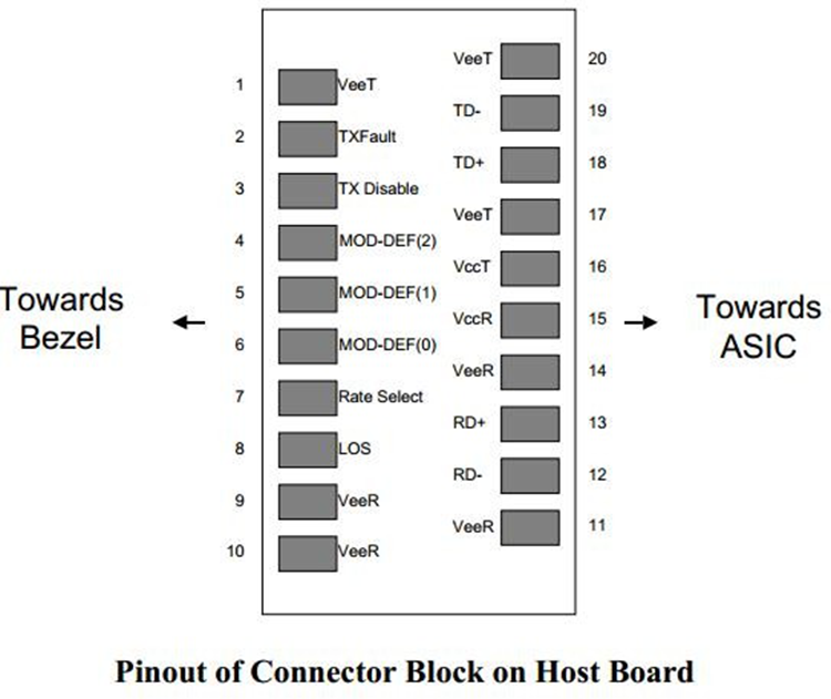
DSFP Pin description
|
Pin |
Descriptions |
Pin |
Descriptions |
|
1 |
VEET |
Transmitter Ground (Common with Receiver Ground) |
1 |
|
2 |
TFAULT |
Transmitter Fault. |
2 |
|
3 |
TDIS |
Transmitter Disable. Laser output disabled on high or open. |
3 |
|
4 |
MOD_DEF(2) |
Module Definition 2. Data line for Serial ID. |
4 |
|
5 |
MOD_DEF(1) |
Module Definition 1. Clock line for Serial ID. |
4 |
|
6 |
MOD_DEF(0) |
Module Definition 0. Grounded within the module. |
4 |
|
7 |
Rate Select |
No connection required |
|
|
8 |
LOS |
Loss of Signal indication. Logic 0 indicates normal operation. |
5 |
|
9 |
VEER |
Receiver Ground (Common with Transmitter Ground) |
1 |
|
10 |
VEER |
Receiver Ground (Common with Transmitter Ground) |
1 |
|
11 |
VEER |
Receiver Ground (Common with Transmitter Ground) |
1 |
|
12 |
RD- |
Receiver Inverted DATA out. AC Coupled |
|
|
13 |
RD+ |
Receiver Non-inverted DATA out. AC Coupled |
|
|
14 |
VEER |
Receiver Ground (Common with Transmitter Ground) |
1 |
|
15 |
VCCR |
Receiver Power Supply |
|
|
16 |
VCCT |
Transmitter Power Supply |
|
|
17 |
VEET |
Transmitter Ground (Common with Receiver Ground) |
1 |
|
18 |
TD+ |
Transmitter Non-Inverted DATA in. AC Coupled. |
|
|
19 |
TD- |
Transmitter Inverted DATA in. AC Coupled. |
|
|
20 |
VEET |
Transmitter Ground (Common with Receiver Ground) |
1 |
Small Form-factor Pluggable (SFP) Transceiver MultiSource Agreement (MSA)
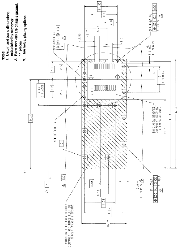
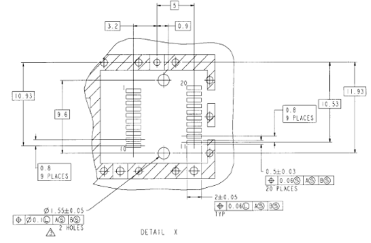
SFP Host Board Mechanical Layout
Figure 6 SFP Host Board Mechanical Layout (Cont.)
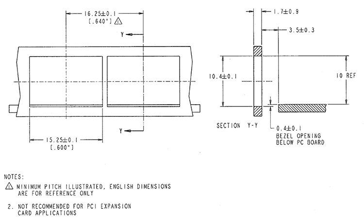
Recommended Bezel Design
Product detail pictures:
Related Product Guide:
Mako Networks’ New 6600 Series Appliances Are Available Now | Sfp Gpon Onu
Semtech Corp (SMTC) Q1 2020 Earnings Call Transcript | Sfp Gpon Onu
With our rich experience and considerate services, we have been recognized as a reliable supplier for many international buyers for Single Core Sfp Module - 155m Lc 1310nm Dual Fiber 20km Fiber Optic Transceiver Sfp Module – HDV , The product will supply to all over the world, such as: Stuttgart, Croatia, Victoria, Due to good quality and reasonable prices, our products have been exported to more than 10 countries and regions. We are looking forward to cooperating with all customers from at home and abroad. Moreover, customer satisfaction is our eternal pursuit.
Factory equipment is advanced in the industry and the product is fine workmanship, moreover the price is very cheap, value for money!


